{{ title }}
{{ category }}
Role: Project Lead · Team: 5 · Timeline: 5 months

Overview
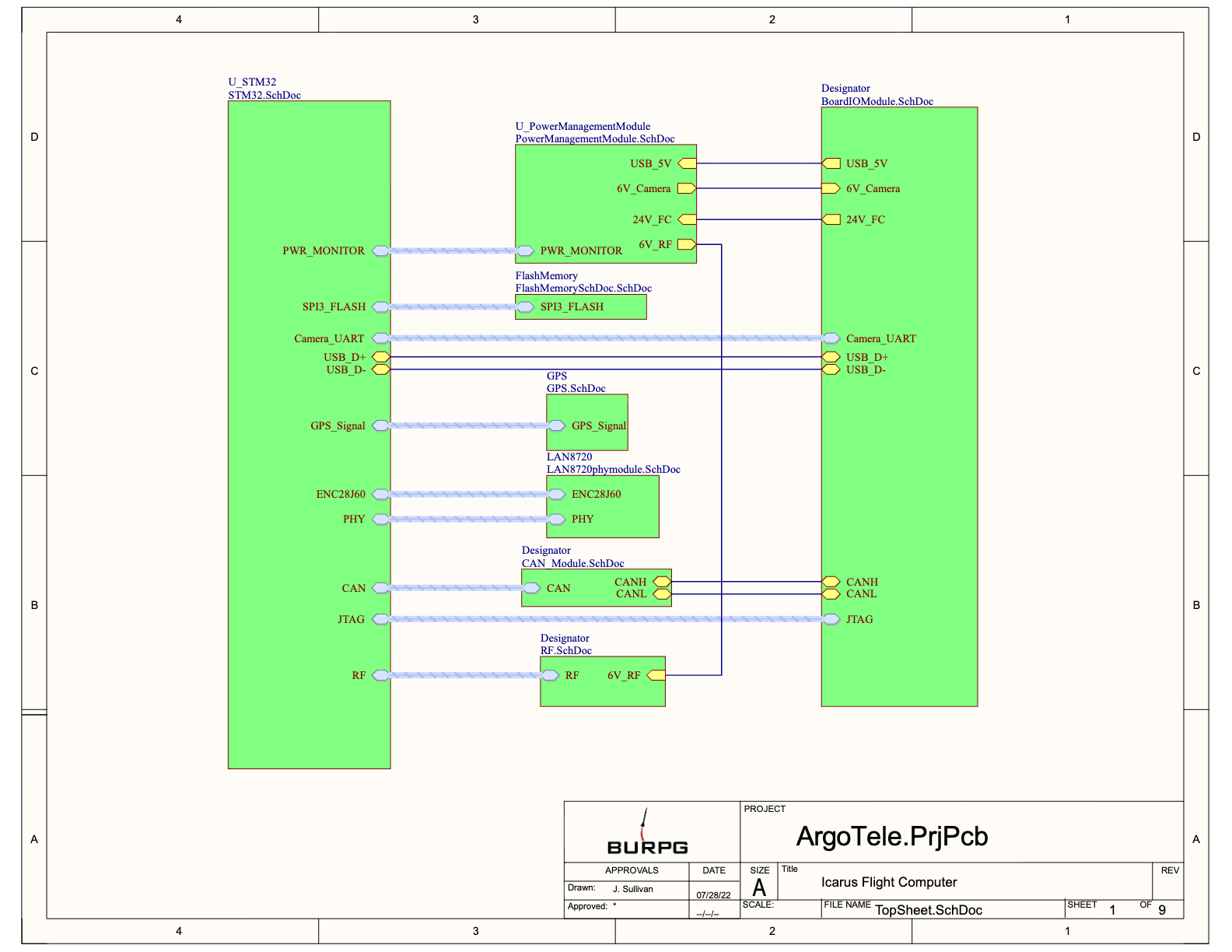
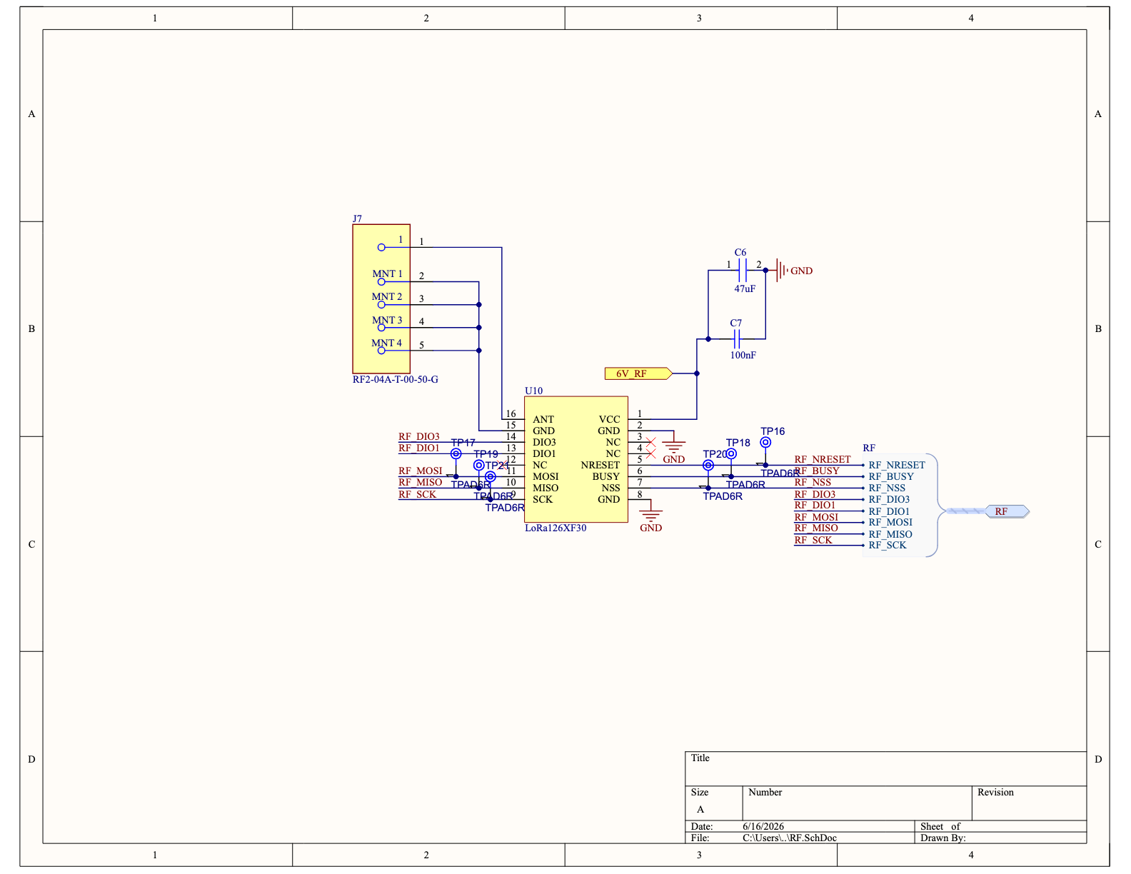
A four-layer telemetry board, 1 of a 3 part system for the Boston University Rocket Propulsion Group's next rocket flight computer with RF ground communication, ethernet, IMU, altimeter, GPS, flash storage, and CAN functionality.
My Role
- Owned schematic capture for the entire board: 9 sheets covering power, RF, Ethernet PHY, GPS, CAN, and flash. Re-used circuits proven on the flight computer board and designed new ones in areas that needed improvement.
- Before starting PCB design, I led a formal design review of the schematic to validate the approach.
- Led PCB layout across a team of 3 new BURPG members: split the board by module, set placement/routing constraints, personally laid out power, USB, flash, and a large part of the Ethernet PHY.
Tools & Tech
Telemetry Board System Role
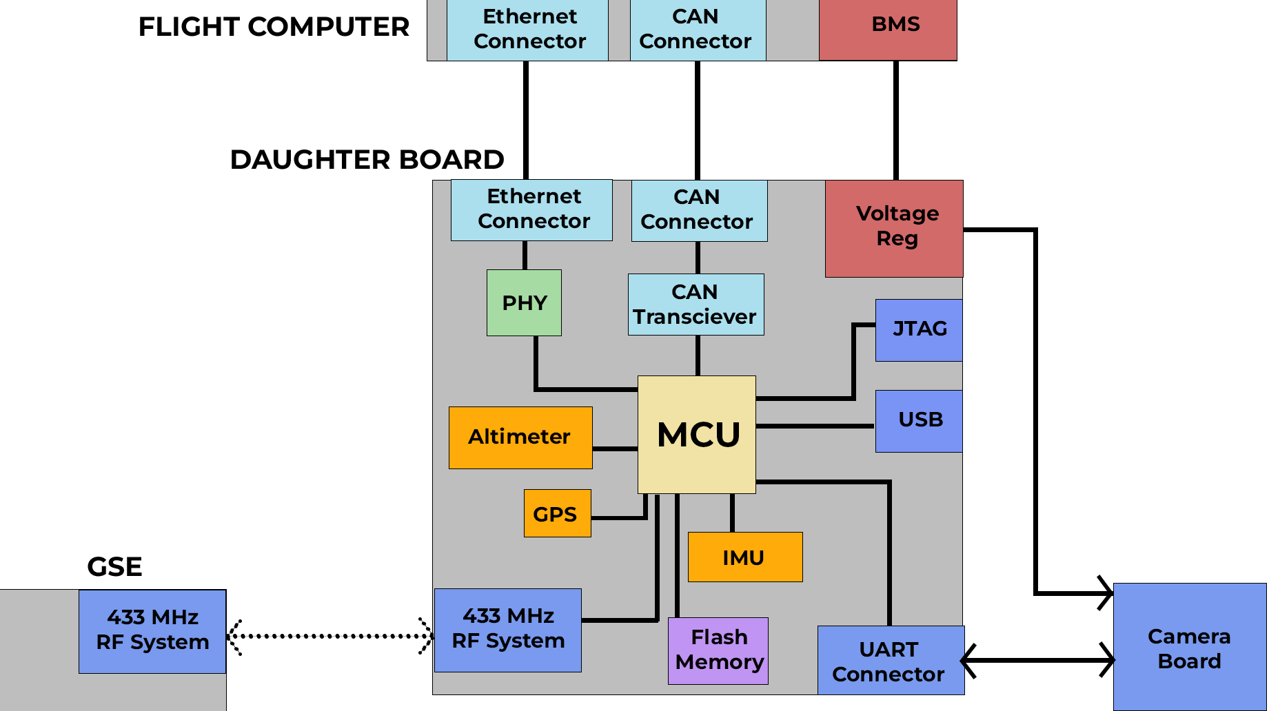
The flight computer for the rocket was designed to have 3 boards in total. It was decided by the team that the first, main flight computer board would have the minimum possible functionality for the rocket to fly in any capacity, while the daughter board or the "telemetry board", would accomplish the following goals:
- RF Communication with Ground Support Electronics
- Power and Control Camera
- House Backup Altimeter and IMU
- House GPS Module
- Critical communications with flight computer board via CAN
- Higher speeds + larger data transfers with flight computer board via Ethernet
Board ICs and why they were chosen
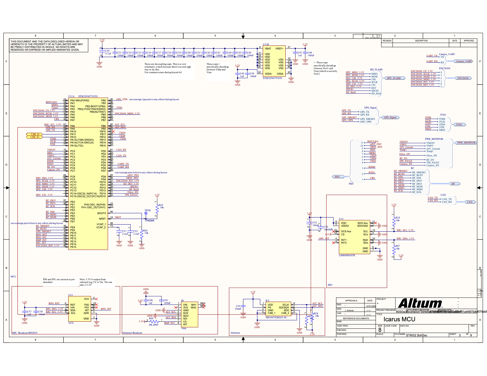
BNO0559-axis, gives absolute orientation in quaternions but updates slower and readings get sketchy under high vibration. Also serves as a known working backup circuit.
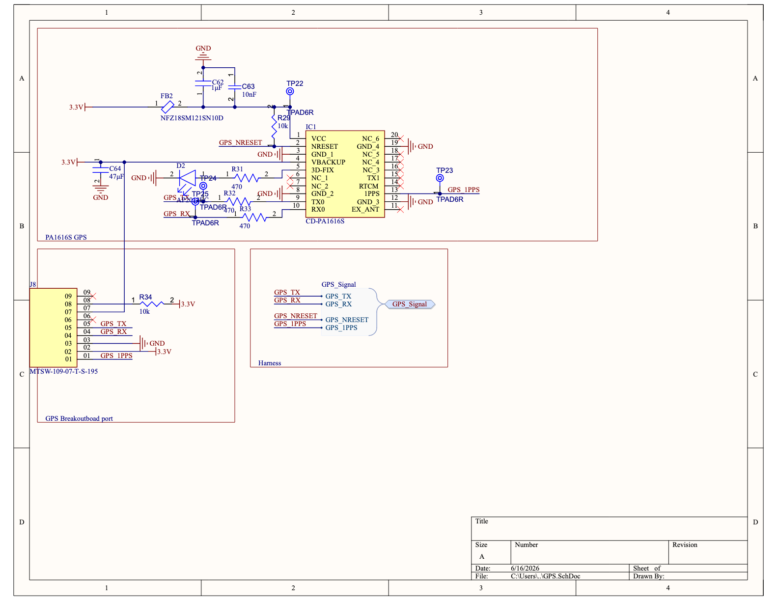
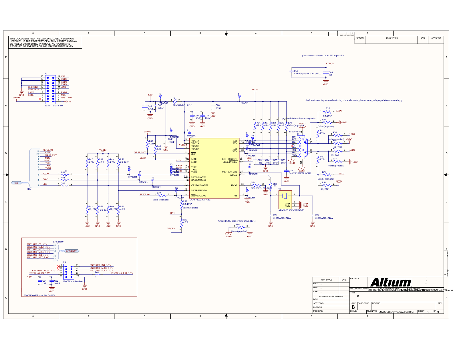
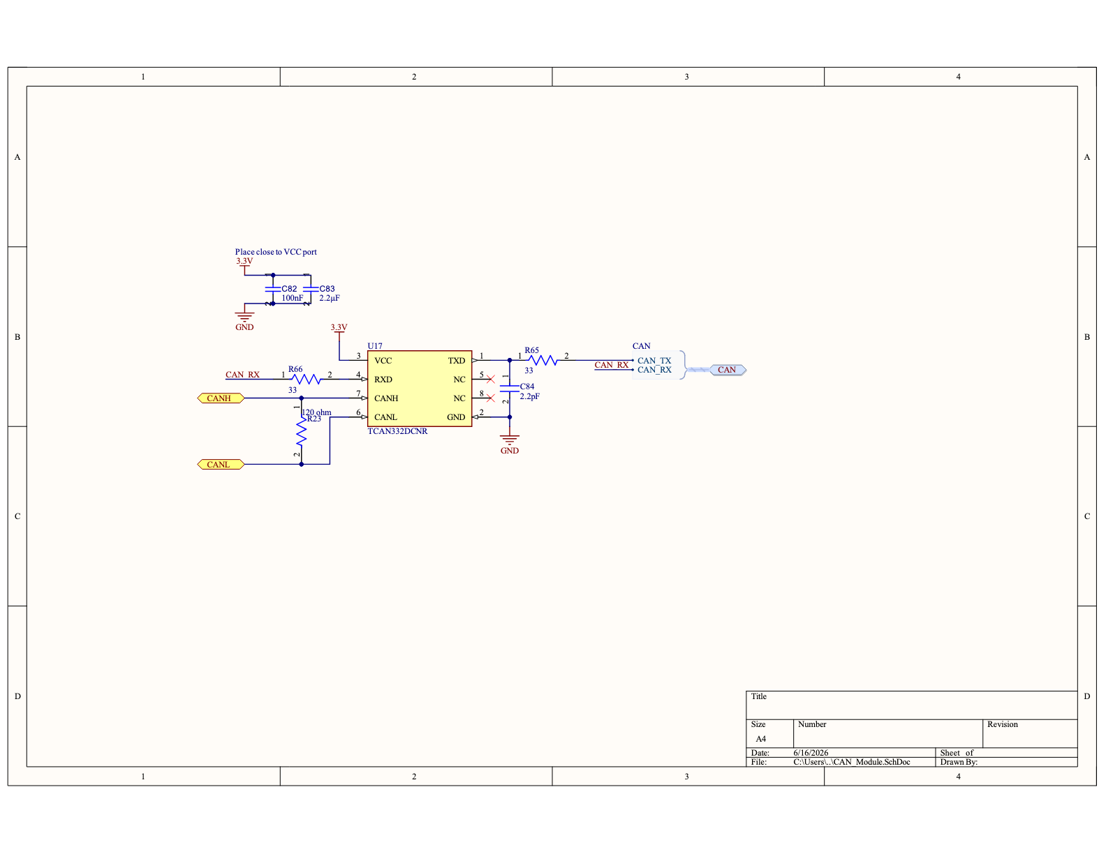
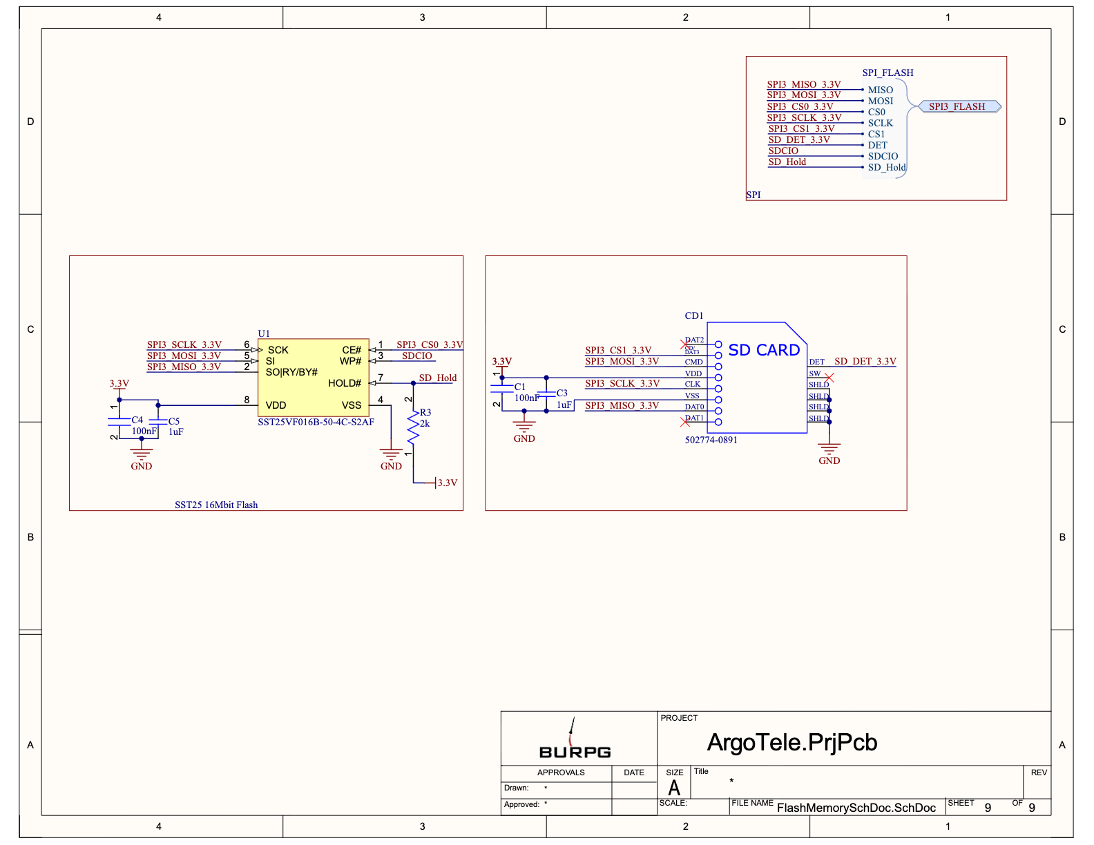
Power Design
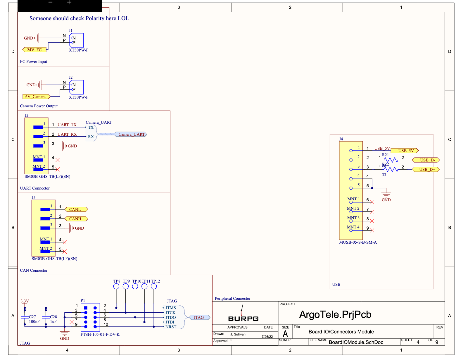
Power comes from XT30 connectors from the flight computer at 24V, and is stepped down by a buck converter to ~6V to power RF and camera modules, and stepped down again by an LDO to 3.3V to power the rest of the ICs. A main, already tested eFuse configuration on the 24V line serves as an extreme backup, protecting upstream flight computer. Tighter current limits are set by the 6V current limiter, and the design also features load switches to control power to camera and RF.
24V to 6V Buck Converter
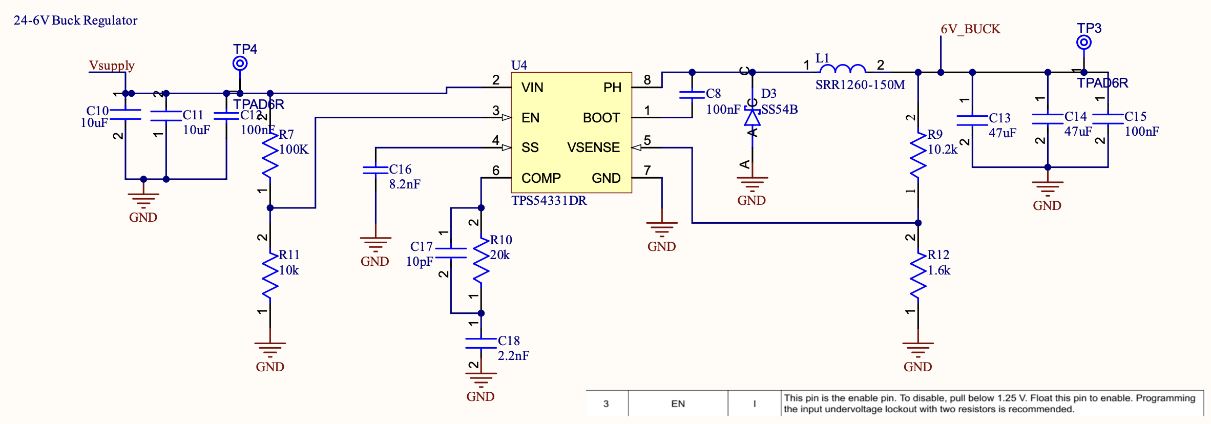
Buck converter chosen for efficiency at a large voltage step-down, powers RF and camera modules. Copied from flight computer 24V to 5V buck, output changed by changing R5 and R6:
0.8V × (10.2k/1.6k + 1) = 5.9V
6V to 3V LDO
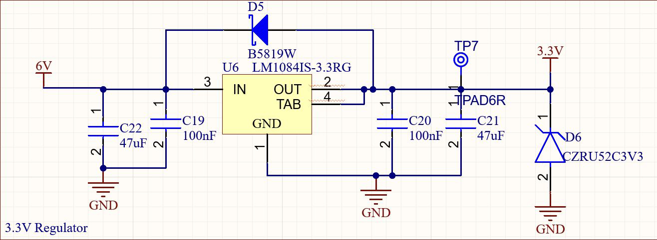
Copied from flight computer 5V to 3.3V converter, nothing changed since output is static at 3.3 V, and design is still within maximum |Vout-Vin| = 27V and minimum |Vout - Vin| = 1.5V.
24V Rail Protection
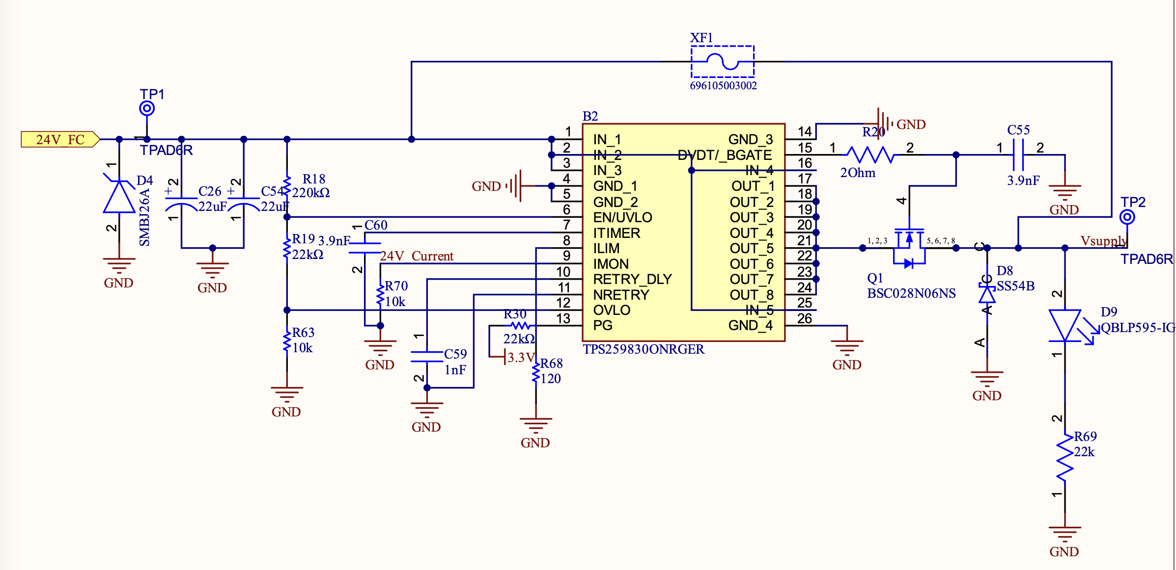
Copied from previous designs, protects upstream system from overcurrent, and protects entire system from overheating and short-circuits.
6V Rail Protection
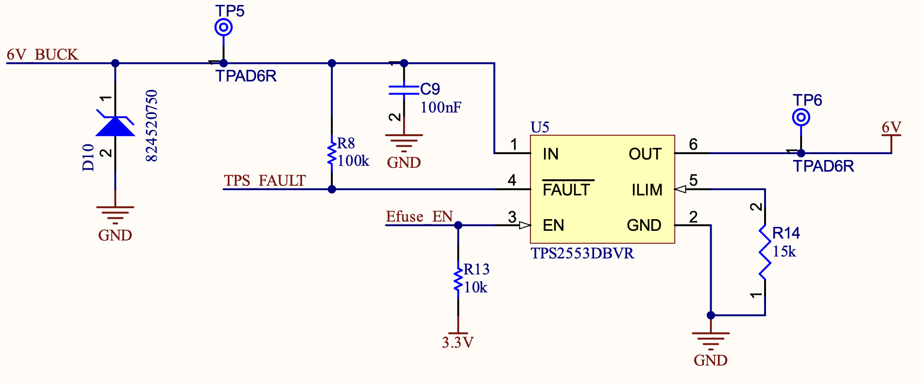
7V maximum input for TPS2553, so D10 has 6.8V reverse breakdown voltage. Current limit is set to ~1.7A, slightly above approximate current draw of system.
Voltage/Temp Monitoring
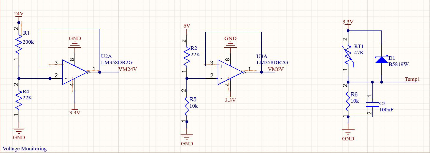
Voltage dividers needed for output voltage values to fit within 3V analog input limit on STM32. Expected output calculated based on input voltage and corresponding dividers.
Load Switches
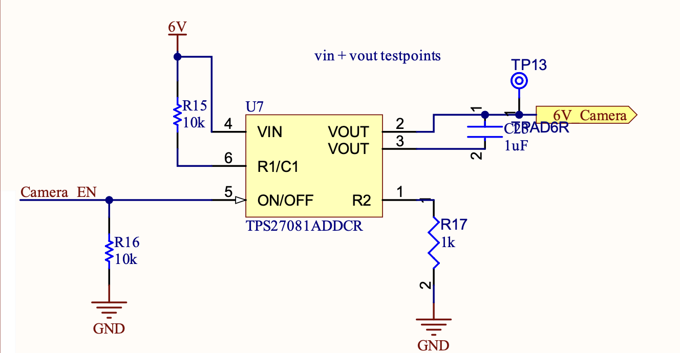
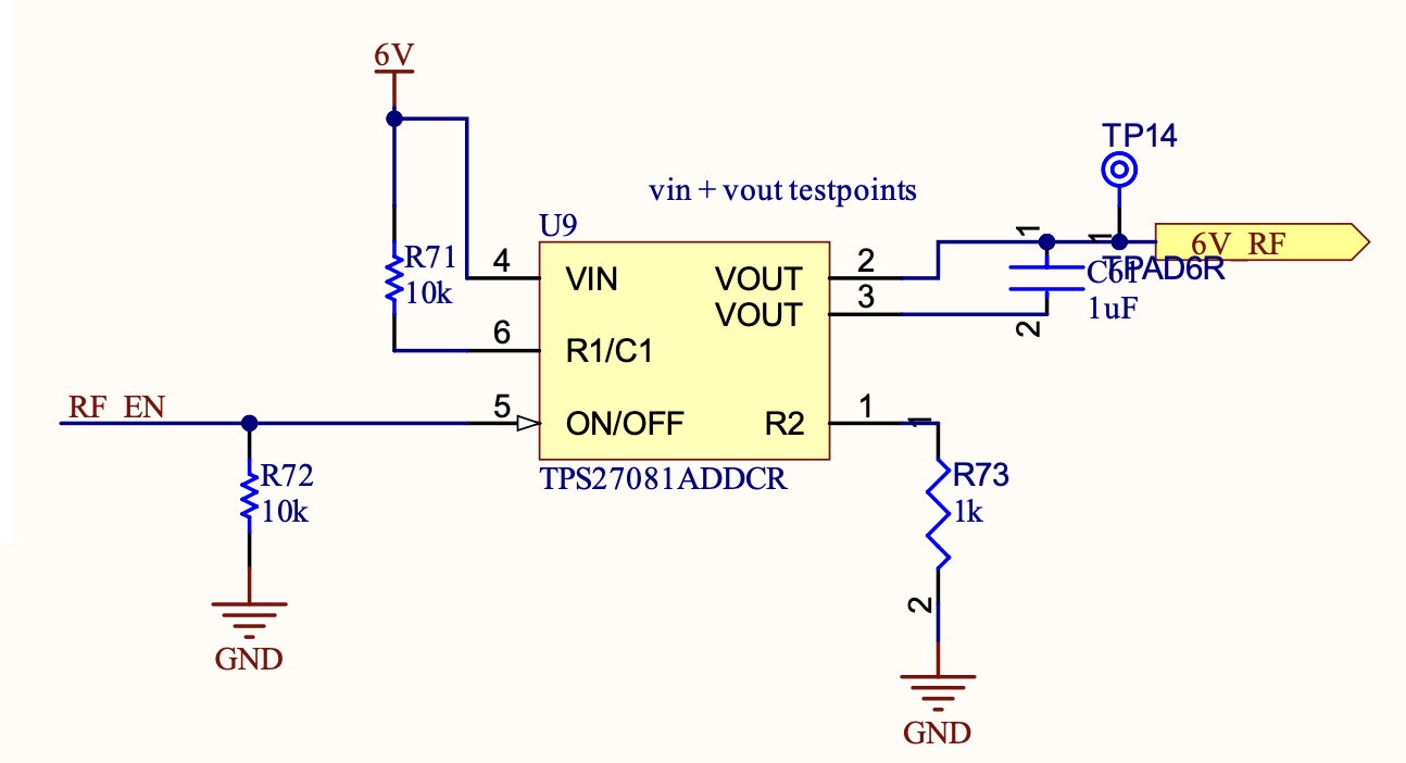
Load switches for camera and RF modules to conserve battery power and subsystem restart functionality, both off by default, turned on by pulling EN signal high. 1uF capacitor on output slows voltage rise, prevents extreme inrush current.
Debugging & Backups
PCB Layout, Team Management, and What I Learned.
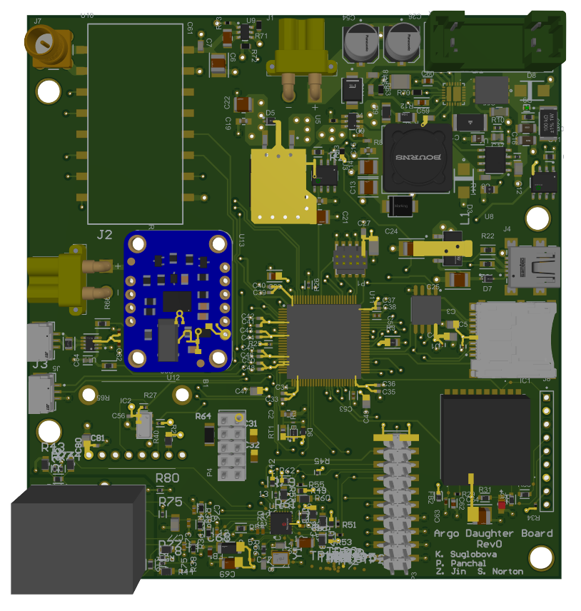
Overview
I owned the schematic through design review, then ran layout with a team of 3. First, I made a draft of where the components would be placed on the board according to size, and then assigned junior team members easier modules (Altimeters, IMUs, GPS, RF) and oversaw their layout. I did this in two stages: the first check was when they physically placed the components on the board, and the next check was after they had routed the traces. After their components were done, some of the members also helped me with connecting all of the ICs to the MCU, which I saved for last in case any last minute placement changes needed to be made. I did the power layout myself, since it was the most complex and simultaneously mission critical, and ended up doing the PHY, as well as the flash and CAN modules. The schematics and PCB for this project were all pushed to a communal git repository, and a version control schedule had to be implemented for the PCB work time.
Setbacks
The schematic process for the board was relatively straightforward, since I had discussed clear requirements with the avionics team, had a person on the electrical team to mentor me that I had worked with prior, and had already had experience with schematics (and layout) for the first flight computer board, which had a similar structure. However, managing a team unraveled a whole new set of challenges.
First off, I ran into an issue with the Altium software itself. Many of the component footprints were acquired from previous designs, which I had locally saved onto my computer, but did not appear for other members when they pulled from Phabricator and opened the PCB layout. This hindered the initial start date, and I had to quickly come up with a fix. Instead of relocating components batch by batch from all separate projects, I found that if I just dragged all of the components onto the PCB board myself and pushed the project, the other team members were able to see them. Therefore, I created a separate section of the board to drag unplaced components, from which my team sourced them.
Secondly, the junior engineers that volunteered to help me with the project were all different skill levels, and this is something I did not realize at the start of the project but should have evaluated. This meant that the same amount of instructions could work for one team member, while the same amount would not work for the other members and would cost much more time for both me and them due to numerous revisions. It also occurred to me that even though I would say something to one member in the presence of the others, it did not mean that the rest of the members would also take that advice, and therefore there were a lot of instructions that needed to be repeated.
Next time, I would make a document with all of the basic PCB guidelines that the entire team could refer to, and go through it with each one individually, and even sit down with them while they do some very basic layout, to make sure they understand the material and can actively implement it, which would save a lot of time.