{{ title }}
{{ category }}
Role: ADC and Ethernet Switch Schematic/Layout · Team: 2 · Timeline: 3 months
Overview
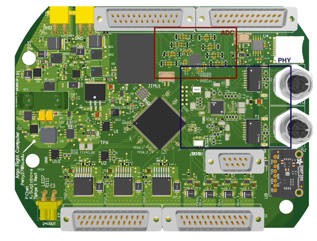
PCB design for the base board of the flight computer of Boston University Rocket Propulsion Group’s latest rocket, Argo. The new flight computer contains CAN, Ethernet, I²C, and SPI communication, flash storage, an altimeter, an IMU, and the power system.
My Role
- Designed the schematics for the analog-to-digital converter and the Ethernet switch modules in Altium.
- Integrated them with the STM32 microcontroller and laid out the components and PCB traces to minimize noise and EMI.
- Fixed design rule check violations and performed manufacturing checks for the whole board.
- On the software side, wrote bare-metal C for the AD7173 when no usable library was available, and confirmed ADC and SPI functionality.
Tools & Tech
Analog-to-Digital Converter
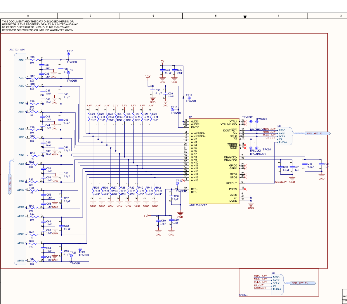
The ADC configuration on previous flight computers used two separate 8 input ADCs (AD7193s) on the same SPI bus in order to get sensor data readings. The new module I chose, the AD7173, had 16 analog inputs, and also had increased sampling speed and better documentation, all for a similar price.
Many analog inputs are needed because the noise levels on flight computers are extremely high, and therefore its extremely beneficial to use differential pairs in order to conserve the signal. Therefore, in each pair of analog inputs, one was tied to VDD, and one was tied to GND. During PCB layout, I impedance-matched these analog pairs. Additionally, many filtering caps were put on the voltage inputs to mitigate noise, and others were put as the documentation required, which were also put close to the module during layout. It was configured to interact with the flight computer via SPI bus.
Our team ran into trouble using publicly available AD7173 libraries to configure the new ADC. Therefore, one software team member continued to search for available libraries, while I started writing C code that would accomplish basic SPI bus functionality and mode setup by manually writing to the registers according to the data sheet. This involved using the J-link to flash and communicate with the STM32, and setting breakpoints in the code and reading register values using PlatformIO, since there was no serial port available (this was fixed on the board I designed later and a USB port was added, since no serial debugging was... rough). In the end, I was able to verify that the PCB layout was correct and that the SPI bus was functioning and the ADC was receiving data, before the team finally found a usable library with pre-built functions for all the settings, which made usage much easier.
Ethernet Switch / PHY
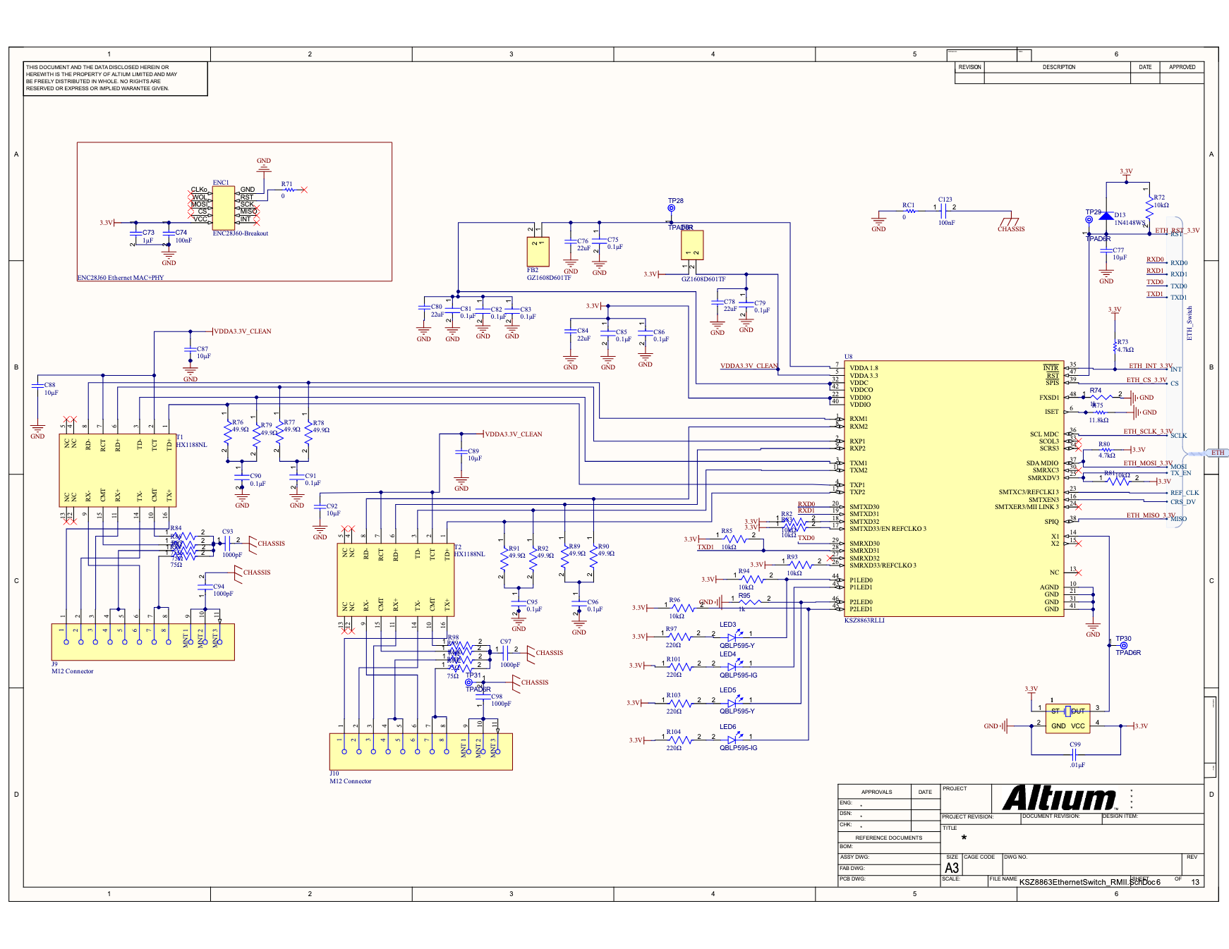
Previous BURPG flight computers all had PHY ICs on board, but they always had hardware issues and were not able to be fully brought up. For this board, we decided to once again put a PHY on board in order to establish ethernet connectivity as an additional, faster method of communication. Except, this time the PHY was an ethernet switch, which, on top of having PHY functionality, switches between two ethernet signals. This functionality was desired due to the multi-board layout of the flight computer, since not only did the MCU need to be able to receive ethernet signal from ground electronics, but it also needed to connect to the other flight computer board.
To simplify bringup as much as possible due to prior issues with ethernet, I decided to put the ethernet switch into RMII mode, which uses half as many signals, and set it to auto-negotiation by default, which eliminates a lot of coding complexity. Instead of standard RJ45 connectors with built-in magnetics, I had to use M12 connectors due to their noise resistance (since this thing is on a rocket). This meant that I had to find separate magnetics and integrate them into the system (HX1188). Also, due to prior issues, I additionally incorporated an ENC28J60 breakout board onto the SPI bus, which has been known to work for the team and allows for ethernet functionality even if something were to go wrong with the switch.